TSMC and Samsung committed to ASML's High-NA EUV scanners, Samsung by 2028 and TSMC by 2030, closing the question of whether the leading foundries would adopt the tool. Intel is already running it. The same week all three joined an ASML initiative to move photomasks from 6-inch to 12-inch, targeting a pilot line in 2031 — because today's mask size costs High-NA about 30% of its throughput.
All three leaders reached 2nm-class volume in 2025, but TSMC holds about two-thirds of the foundry market and spends ~$40B a year to keep it. IBM demonstrated a sub-1nm transistor in 2026 — a research result roughly five years from production.
ASML lifted 2026 revenue guidance to €43–45B (from €36–40B, +16% at midpoint) after a Q2 beat (€9.33B revenue, €2.92B net), and will expand low-NA EUV and DUV immersion capacity by 30% each. Intel becomes the first to make chips (Panther Lake) on its High-NA tool.
A single advanced fab costs $20–30B and depends on EUV machines only ASML makes. That brutal economics narrows the frontier to a handful of firms — and makes leading-edge capacity one of the world's true chokepoints.

 TSMC
TSMC  Intel
Intel 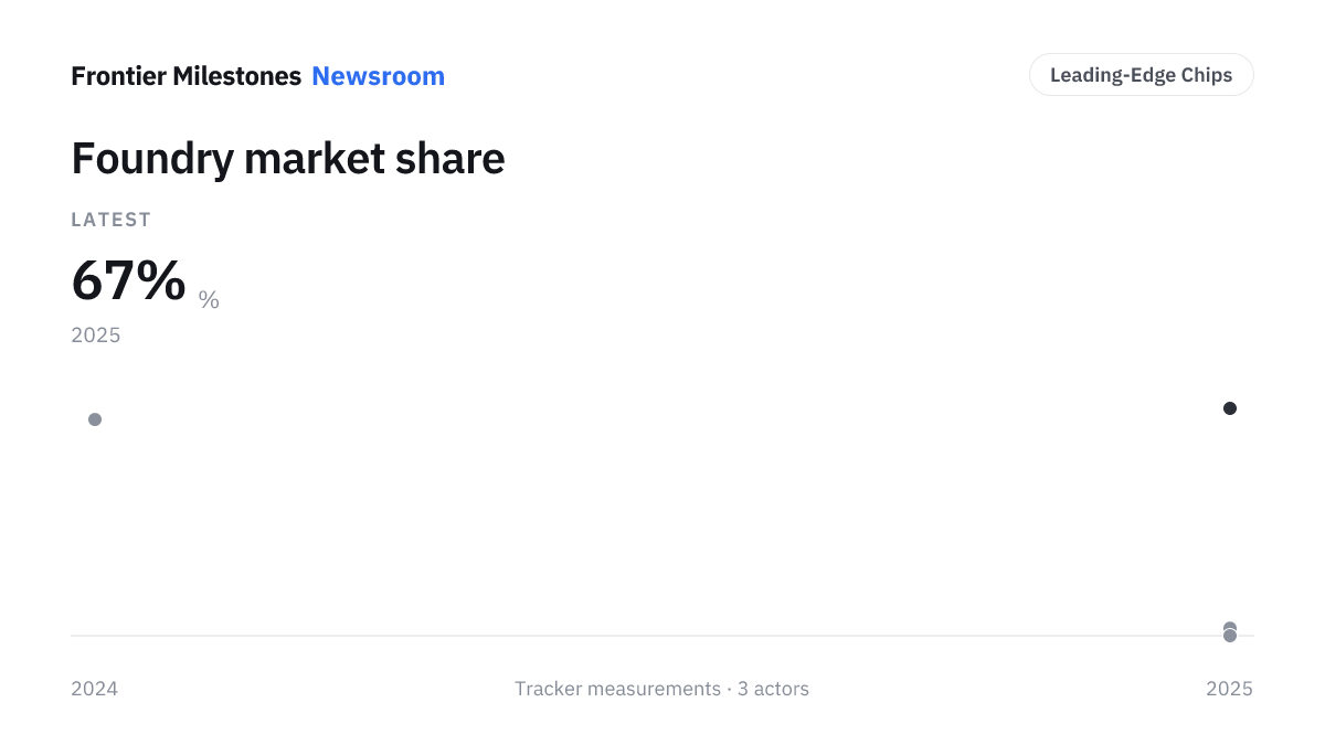
 Samsung Foundry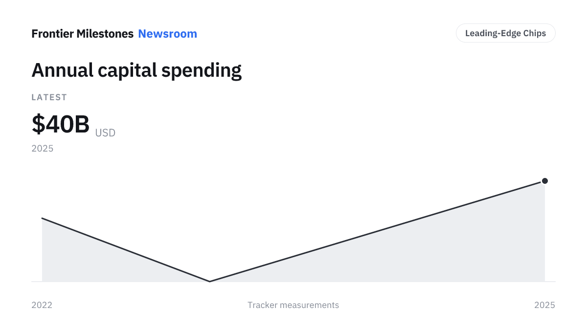
 SMIC
SMIC