TSMC and Samsung committed to ASML's High-NA EUV scanners, Samsung by 2028 and TSMC by 2030, closing the question of whether the leading foundries would adopt the tool. Intel is already running it. The same week all three joined an ASML initiative to move photomasks from 6-inch to 12-inch, targeting a pilot line in 2031 — because today's mask size costs High-NA about 30% of its throughput.
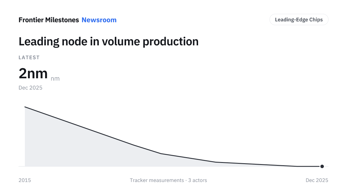
All three leaders reached 2nm-class volume in 2025, but TSMC holds about two-thirds of the foundry market and spends ~$40B a year to keep it. IBM demonstrated a sub-1nm transistor in 2026 — a research result roughly five years from production.
Herald Economy reported that SK hynix is considering Intel Foundry as a second source for the base dies under its HBM4E stacks, work that currently runs entirely through TSMC. SK hynix said it is not currently considering Intel for HBM4E, calling parts of the report inaccurate without specifying which.
The two will capitalize Advanced Vision Semiconductor Manufacturing Corp with ¥465B from Sony (cash plus its new Kumamoto fab) and ¥282B from TSMC — about $4.69B combined. Sony controls the venture and leads sensor technology and design; TSMC supplies advanced process technology. Volume production is targeted for 2029.
TSMC's Q2 net profit jumped 77% year on year to a record NT$706.6B (~$22B), far beating estimates. It raised 2026 capex guidance to $60–64B (from $52–56B), lifted its revenue growth forecast to over 40%, and pledged an additional $100B for Arizona — bringing total US commitments to about $265B.
TSMC holds ~two-thirds of the market and the yield lead; Intel is betting its comeback on 18A; Samsung trails on yield. Our read on a race where one player's dominance keeps compounding. (Our opinion, not investment advice.)
Our read — labelled opinion, not investment advice.
A single advanced fab costs $20–30B and depends on EUV machines only ASML makes. That brutal economics narrows the frontier to a handful of firms — and makes leading-edge capacity one of the world's true chokepoints.
No part of a "2nm" chip is 2 nanometers. Node names are marketing labels, not physical measurements — so we read them alongside transistor density and who is actually shipping in volume.

 ASML
ASML  Intel
Intel 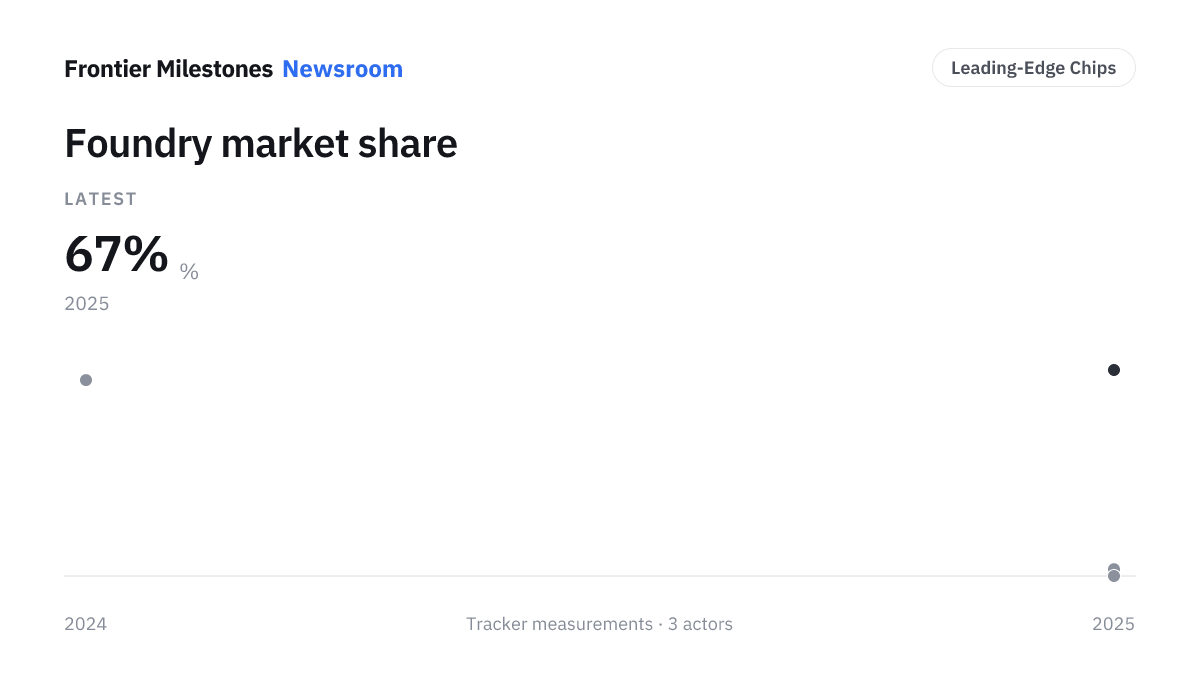
 Samsung Foundry
  SK hynix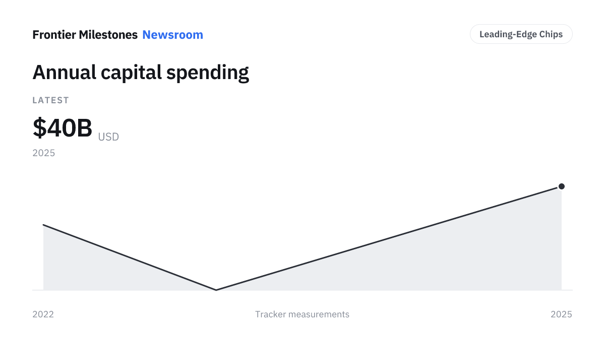
 SMIC
SMIC